Chapter 5: Difference between revisions
Jump to navigation
Jump to search
No edit summary |
|||
| Line 6: | Line 6: | ||
*'''JFET''': Charge flows through a semiconducting channel (between the source and drain). Applying a bias voltage to the gate terminal impedes the current flow (or pinches it off completely). <math>V_{to}</math> is the opposite polarity of the Enhancement mode. |
*'''JFET''': Charge flows through a semiconducting channel (between the source and drain). Applying a bias voltage to the gate terminal impedes the current flow (or pinches it off completely). <math>V_{to}</math> is the opposite polarity of the Enhancement mode. |
||
===Modes of operation=== |
===Modes of operation=== Change so that this is not just for n-channel enhancement |
||
[[Image:MOS-Transistors-NMOS-and-PMOS.jpg|thumb|450px|NMOS & PMOS in Cutoff ]] |
[[Image:MOS-Transistors-NMOS-and-PMOS.jpg|thumb|450px|NMOS & PMOS in Cutoff ]] |
||
[[Image:NMOS-Transistors-Operation.png|thumb|450px| Triode (Linear) and Saturation (B.P.O = Beyond Pinch Off)<br>NMOS]] |
[[Image:NMOS-Transistors-Operation.png|thumb|450px| Triode (Linear) and Saturation (B.P.O = Beyond Pinch Off)<br>NMOS]] |
||
| Line 79: | Line 79: | ||
#Use the small-signal equivalent circuit to find the impedance and gains |
#Use the small-signal equivalent circuit to find the impedance and gains |
||
===Small-signal equivalent circuits=== |
===Small-signal equivalent circuits=== Insert photo |
||
*"Transconductance, g<sub>m</sub>, is an important parameter in the design of amplifier circuits. In general, better performance is obtained with higher values of g<sub>m</sub>."<ref>Electroincs p. 310</ref> |
*"Transconductance, g<sub>m</sub>, is an important parameter in the design of amplifier circuits. In general, better performance is obtained with higher values of g<sub>m</sub>."<ref>Electroincs p. 310</ref> |
||
*Transconductance is defined as <math>g_m=2K(V_{GSQ}-V_{to})=\sqrt {2KP} \sqrt {W/L} \sqrt{I_{DQ}}</math>. |
*Transconductance is defined as <math>g_m=2K(V_{GSQ}-V_{to})=\sqrt {2KP} \sqrt {W/L} \sqrt{I_{DQ}}</math>. |
||
| Line 97: | Line 97: | ||
===Questions=== |
===Questions=== |
||
*What's the difference between the enhancement and depletion modes? |
|||
*NMOS and BJTs seem very similar. Why would you use one over the other? |
|||
*How do you find r<sub>d</sub>? |
*How do you find r<sub>d</sub>? |
||
*Roughly what are the breakdown voltages for JFETs? |
*Roughly what are the breakdown voltages for JFETs? |
||
*Learn how to check for operating regions via V<sub>gs</sub> & V<sub>ds</sub> as compared to V<sub>to</sub>. |
|||
*CMOS nand/nor gates |
*CMOS nand/nor gates |
||
*JFET only goes to I<sub>DSS</sub> |
*JFET only goes to I<sub>DSS</sub> |
||
*Small signal model of mosfets |
|||
===References=== |
===References=== |
||
Revision as of 17:57, 19 March 2010
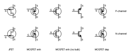
Metal-oxide semiconductor field effect transistor (MOSFET)
"In MOSFETs, a voltage on the oxide-insulated gate electrode can induce a conducting channel between the two other contacts called source and drain. The channel can be of n-type or p-type, and is accordingly called an nMOSFET or a pMOSFET (also commonly nMOS, pMOS)."<ref>http://en.wikipedia.org/wiki/MOSFET MOSFET - Wikipedia</ref>
- Enhancement: The electric field from the gate voltage forms an induced channel allowing current to flow.
- Depletion: The channel is physically implanted rather than induced. Thus, is the opposite polarity of the Enhancement mode.
- JFET: Charge flows through a semiconducting channel (between the source and drain). Applying a bias voltage to the gate terminal impedes the current flow (or pinches it off completely). is the opposite polarity of the Enhancement mode.
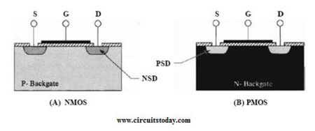
===Modes of operation=== Change so that this is not just for n-channel enhancement
- Cutoff
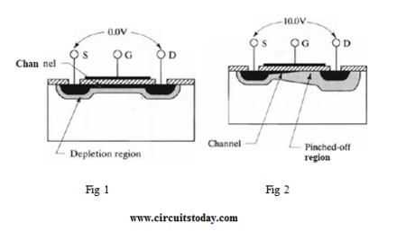
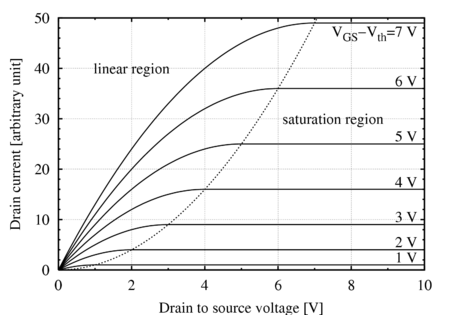
- Triode:
- The threshold voltage, , is the minimum needed to move the transistor from the Cutoff to Triode region. When is reached, a channel forms beneath the gate, allowing current to flow.
- is usually on the order of a couple of volts
- For small values of , is proportional to . The device behaves as a resistor whose value depends on
- Saturation:
- "Now consider what happens if we continue to increase . Because of the current flow, the voltages between points along the channel and the source become greater as we move toward the drain. Thus, the voltage between gate and channel becomes smaller as we move toward the rain, resulting in a tapering of the channel thickness as illustrated in Figure 5.5. Because of the tapering of the channel, its resistance becomes larger with increasing , resuling in a lower rate of increase of ." <ref>Electronics p. 291</ref>
Device equations
|
| |||||||||||||||||||||||||||
| Region | (Enhancement/Depletion) |
(JFET) | |
|---|---|---|---|
| Cutoff | |||
| Triode | |||
| Saturation | |||
| Boundry |
- Device Parameters:
- Surface Mobility: , the electrons in the channel
- Capacitance of the gate per unit area:
Pros and Cons
| Transistor | Pros | Cons |
|---|---|---|
| MOSFET | Draws no gate current Infinite input resistance |
Gate protection needed to prevent static electricity from breaking down the insulation |
| JFET | ||
| BJT |
Analysis
- Analyze the DC circuit to find the Q-point (using nonlinear device equations or characteristic curves)
- Use the small-signal equivalent circuit to find the impedance and gains
===Small-signal equivalent circuits=== Insert photo
- "Transconductance, gm, is an important parameter in the design of amplifier circuits. In general, better performance is obtained with higher values of gm."<ref>Electroincs p. 310</ref>
- Transconductance is defined as .
- , where rd is the drain resistance
| Type | Voltage Gain | Current Gain | Power Gain | Input Impedance | Output Impedance | Frequency Response |
|---|---|---|---|---|---|---|
| Common-Source | High | Low | ||||
| Source Follower | ||||||
| Common-Gate |
Questions
- How do you find rd?
- Roughly what are the breakdown voltages for JFETs?
- CMOS nand/nor gates
- JFET only goes to IDSS
References
<references/>


![{\displaystyle K[2(v_{GS}-V_{to})v_{DS}-v_{DS}^{2}]}](https://wikimedia.org/api/rest_v1/media/math/render/svg/40bb5b0ffa3dcb84c09c7252ed8fc731f03619f2)


