Dynamic Carrier Control
for the RCA BHF-100B Transmitter
Rob Frohne
School of Engineering
Walla Walla College
204 S. College Avenue
College Place, WA 99324
Internet: frohro@wwc.edu
Phone: (509) 527-2075
Fax: (509) 527-2867
This document describes the dynamic carrier control circuitry for the
RCA BHF 100B transmitter. Dynamic carrier control (DCC) is a means of making
amplitude modulation more efficient. The object is to reduce the energy
consumption of the AM transmitter without degrading the performance. When
modulation is low, the amount of carrier power required to transmit the
AM signal is less than when the modulation is high. DCC controls the carrier
power dynamically as the modulation changes. The particular type of dynamic
carrier control used in this implementation was developed by Asea Brown
Bavari (ABB) and is described in their publication number CH-E 3.10814.1E
which is included in this documentation as Appendix 1. In this scheme the
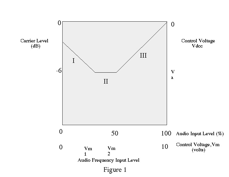
carrier level is adjusted as a function of the audio level as shown in
Figure 1. In region III the carrier is dropped in direct proportion to
the audio input so that the transmitter is 100% modulated. In region II
the carrier is kept at the same level so that if the modulation stayed
in this region it would act like a standard AM transmitter. The carrier
is increased in region I so that co-channel interference is less evident
during soft passages of audio.
Operation
There are only three switches used to operate the DCC circuitry. This
section describes what they do. The DCC interfaces to the IPA drive control
circuit as well as the phase modulators. Either or both of these interfaces
may be switched out. (If both of them are switched out, the DCC is not
active.) Since it has been common practice with the transmitters to tune
them so that either channel one or channel two is 135 degrees ahead of
the other there is also a phase reversal switch which allows the DCC phasing
interface to compensate for this. The DCC phase reversal switch (SW2) and
the DCC phasing interface disable switch (SW1) are located in the upper
right hand corner of the exciter. The DCC IPA drive control disable switch
(SW3) is located by the drive balance control to the left of the exciter.
WARNING! It is important to be sure that the phase reversal switch
(SW2) is set correctly when employing the phase modulator interface
circuitry. If it is not, the DCC circuit will actually cause the transmitter
to use more power than if the DCC was disabled! To ensure that it is
set correctly, observe the final amplifier current during modulation. It
should decrease during lulls in the audio. If it doesn't the phase should
be reversed by switching the phase reversal switch (SW2).
If the transmitter is operating on only one channel for some reason,
only the DCC IPA drive control interface will operate. The DCC phase modulator
interface might as well be switched off.
It is probably best if the final adjustments to the tuning and audio
levels to the transmitter are made when the DCC is switched in so that
the operating conditions are not changed when the DCC is applied.
Circuit Description
This section describes the operation of the DCC circuit. It begins
with an overview of the block diagram and then the operation of each block
is described. It may be helpful to refer to both the block diagram (Figure
2) and the schematic diagram (Figure 3) when reading this section.
Block Diagram
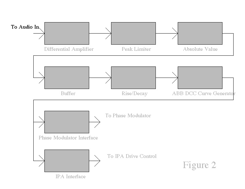 The block diagram of
the circuit is shown in Figure 2, below. Audio is taken from the balanced
audio input to the exciter and converted into a single ended signal by
the differential amplifier. This signal is amplified to a level where the
maximum expected audio signal swings the amplifier into saturation in the
peak limiter. The output of the peak limiter is applied to an absolute
value circuit which is buffered. The result of this is fed into a fast
charge slow discharge circuit that will make the DCC respond quickly to
the need to increase the carrier, but slowly to the need to decrease the
carrier. This result is fed into a circuit whose input/output characteristics
are shown in Figure 1, the ABB DCC curve. The resulting signal is then
interfaced to the transmitter in both the phase modulators and the intermediate
power amplifiers (IPAs).
The block diagram of
the circuit is shown in Figure 2, below. Audio is taken from the balanced
audio input to the exciter and converted into a single ended signal by
the differential amplifier. This signal is amplified to a level where the
maximum expected audio signal swings the amplifier into saturation in the
peak limiter. The output of the peak limiter is applied to an absolute
value circuit which is buffered. The result of this is fed into a fast
charge slow discharge circuit that will make the DCC respond quickly to
the need to increase the carrier, but slowly to the need to decrease the
carrier. This result is fed into a circuit whose input/output characteristics
are shown in Figure 1, the ABB DCC curve. The resulting signal is then
interfaced to the transmitter in both the phase modulators and the intermediate
power amplifiers (IPAs).
The details of each circuit are shown in the schematic diagram, Figure
3, and are described below.
Differential Amplifier
The differential amplifier is a standard one with unity gain and 20
kilo-ohms differential input impedance. Its purpose is to reject common
mode noise present on the balanced input to the exciter.
Peak Limiter
The peak limiter is a standard inverting amplifier which saturates
around +/- 14 volts whose gain can be adjusted from zero to 10. Its purpose
is to insure that if saturation occurs (due to too large an audio input)
anywhere in the circuit, it occurs here. The carrier will be set at the
maximum value when this happens.The one kilo-ohm clipping potentiometer
lowers this voltage down to the proper level so that this happens.
Absolute Value Circuit
This circuit takes the absolute value of the input signal. The 180
kilo-ohm resistor is adjusted so that the positive and negative going peaks
are amplified by the same amount (approximately 0.5).
Buffer Amplifier
The buffer amplifier is necessary because the absolute value circuit
needs to work into a very high impedance for good accuracy. It is a standard
non-inverting buffer amplifier with a gain of 22.
Fast Attack, Slow Decay Circuit
The output of the buffer charges the 1.0 microfarad capacitor through
100 ohms and discharges it through 100 ohms in series with the 1 megohm
potentiometer. This keeps adjacent channel interference due to momentary
over modulation negligible. The time constant for increasing the carrier
is 100 microseconds and the time constant for reducing the carrier is adjustable.
The BBC suggests around 200 milliseconds for this which corresponds to
a potentiometer setting of 200 kilo-ohms.
Asea Brown Bavari Carrier Curve Generator
The Asea Brown Bavari carrier curve generator is by far the most complex
part of the DCC circuit. Refer to Figure 1. If the output from the attack/decay
circuit, Vm, is less than reference voltage Vm1, then the characteristic
of region I is developed; if Vmis between reference voltages Vm1 and Vm2,
the characteristic of region II is developed; if Vm is greater than Vm2,
then the characteristic of region III is developed. Comparators, CMP1 and
CMP2 control the LF13331 analog switches that determine which linear combination
of voltages is summed in the inverting summing amplifiers at the output
of the ABB curve generator. These inverting summing amplifiers have a gain
of 1.50.
Phase Modulator Interface
In channel 1 of the transmitter, the connection between C152 and R135
was severed; switch SW1 serves to either reconnect that connection
or to allow the sum of the audio from C152 and the carrier control voltage
to be applied to R135 which is the input to the phase modulator of channel
one. A similar thing is done with the channel two where the carrier control
voltage is of the opposite sign of that for channel 1. Since it has been
the practice to tune the transmitter up with channel 1 either 135 degrees
ahead or behind channel 2 a phase reversal switch (SW2) allows the phasing
of the DCC control voltages to be reversed.
Intermediate Power Amplifier Interface
Both channels of the IPA drive are controlled simultaneously by adjusting
what used to be the ground point on the bias control from approximately
ground to -14 volts using an non-inverting amplifier driving an N channel
enhancement mode MOSFET which easily handles the few hundred milliamperes
travelling through this network. The diode from drain to source of the
MOSFET is for protection of the MOSFET. R7 sets the amount of IPA bias
control. The amount of control is limited because the op amp saturates
at about -14 volts. Special care was taken in the construction of this
circuit to keep RFI from becoming a problem. The signals from the main
DCC board in the exciter cabinet were shielded and ferrite toroidal RFI
suppressors were added near the main DCC board in the exciter cabinet.
Bypassing capacitors were also necessary on both ends of the shielded cable.
Even with these precautions, the RFI suppression was found to be only barely
adequate. Further measures may be necessary in Palau.
Adjustment and Calibration
The DCC circuit should not require frequent re-alignment. The following
procedure is provided mostly in case another ABB DCC curve is desired,
and so that twiddlers will have a better idea what happens when they tweak
something. It will prove handy to have an oscilloscope, and a function
generator for the alignment of the DCC circuit. The function generator
should be connected to the audio input of the transmitter. To align the
DCC circuit perform the following steps:
1) Measure the amplitude of the audio in at pin 1 of Amp 0 for 100%
modulation of the transmitter. Set R1 so that the waveform at pin 14 of
Amp 0 is just clipping on top and bottom.
2) With the audio input set so that clipping just occurs at pin 14
of Amp 0 set R2 so that the voltage on pin 14 of Amp 1 is 10.0 volts DC.
3) Set Vm1 and Vm2 according to the exact ABB DCC characteristic
you wish to use by adjusting R5 and R6. See Figure 1 to determine exactly
how you would like to place regions I, II and III, which determines the
values for Vm1 and Vm2.
4) With the audio input still set so that clipping just occurs at pin
14 of Amp 0 set Va by adjusting R4 so that Vdcc is 0.0 volts DC.
5) R3 should be around 200 kilo-ohms to start with; however, it may
be adjusted to whatever decay time you wish for lowering the carrier.
Update: 2019
I seem to have lost Figure 3, the schematic diagram. My apologies. This is
a very old circuit. I would not use this type of analog signal processing
these days. I did find a similar
analog circuit
I designed for Adventist
World Radio (KSDA) on Guam in the early 1990's. It was used for a number of
years, and saved them more money than my salary at Walla Walla College back
then.