Chapter 2: Difference between revisions
Jump to navigation
Jump to search
No edit summary |
No edit summary |
||
| (18 intermediate revisions by 3 users not shown) | |||
| Line 1: | Line 1: | ||
=Ideal Op Amp Characteristics= |
|||
*[[Chapter_1#Amplifier_Models | Infinite input impedance]] |
*[[Chapter_1#Amplifier_Models | Infinite input impedance]] |
||
*Infinite open-loop gain for the differential signal |
*Infinite open-loop gain for the differential signal |
||
| Line 6: | Line 6: | ||
*[[Chapter_1#Amplifier_Models | Zero output impedance]] |
*[[Chapter_1#Amplifier_Models | Zero output impedance]] |
||
*Infinite bandwidth |
*Infinite bandwidth |
||
** |
**This means there are no inductors or capacitors in the model and allows for instantaneous changes (and infinite gain regardless of frequency). |
||
=Op Amp Nodal Analysis= |
|||
*[[Chapter_1#Amplifier_Models | No current flows into the + or - terminals]] |
*[[Chapter_1#Amplifier_Models | No current flows into the + or - terminals]] |
||
*If negative feedback is present (and no positive feedback), then <math>V_+ = V_-\,</math> |
*If negative feedback is present (and no positive feedback), then <math>V_+ = V_-\,</math> |
||
*Write nodal equations at <math>V_+\,</math> and <math>V_-\,</math>, but not at <math>V_o\,</math> |
*Write nodal equations at <math>V_+\,</math> and <math>V_-\,</math>, but not at <math>V_o\,</math> |
||
**There is a voltage source inside the op amp. Writing a nodal equation at a voltage source adds an extra equation and an extra variable. |
**There is a voltage source inside the op amp. Writing a nodal equation at a voltage source adds an extra equation and an extra variable. It doesn't make the problem any easier. |
||
=DC imperfections= |
|||
[[Image:DC_Imperfections.PNG |thumb|300px|DC Imperfections]] |
[[Image:DC_Imperfections.PNG |thumb|300px|DC Imperfections]] |
||
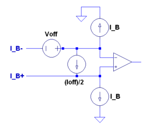
*Bias currents, <math>I_{B+}\,</math> and <math>I_{B-}\,</math>, are the average dc currents flowing into the op amp input terminals. They can be caused by the signal source, feedback resistors, etc. |
*Bias currents, <math>I_{B+}\,</math> and <math>I_{B-}\,</math>, are the average dc currents flowing into the op amp input terminals. They can be caused by the signal source, feedback resistors, etc. |
||
| Line 20: | Line 20: | ||
*Offset current is the difference between the bias currents. <math>I_{off} = I_{B+}-I_{B-}\,</math> |
*Offset current is the difference between the bias currents. <math>I_{off} = I_{B+}-I_{B-}\,</math> |
||
*Offset voltage occurs when the output voltage is nonzero for zero input voltage. |
*Offset voltage occurs when the output voltage is nonzero for zero input voltage. |
||
<br> |
|||
<br> |
|||
<br> |
|||
<br> |
|||
<br> |
|||
<br> |
|||
<br> |
|||
<br> |
|||
==Canceling bias currents== |
|||
*Because bias |
*Because bias current flows have equal magnitude and direction, it is possible to negate their effects. |
||
**The orientation of the offset voltage and the direction of the offset current are unknown, thus it is not possible to correct for these parameters with a circuit design. |
**The orientation of the offset voltage and the direction of the offset current are unknown, thus it is not possible to correct for these parameters with a circuit design. |
||
===Steps=== |
|||
#Ground the input |
#Ground the input |
||
#Set the output to 0 |
#Set the output to 0 |
||
#Add in the bias currents |
#Add in the bias currents |
||
#Add in the new resistor to balance out the |
#Add in the new resistor to balance out the bias currents |
||
#Set the two nodal equations equal to each other and solve for the new resistor |
#Set the two (input terminal) nodal equations equal to each other and solve for the new resistor |
||
=== |
===Reasoning=== |
||
*When the input is grounded, the bias currents will lead to an offset voltage. Arbitrarily setting the output to zero and adding in the bias resistor allows us to have current flowing through the bias resistor equal to even out the bias currents. Due to symmetry, the bias currents will cancel each other out. |
|||
===Problem 2.17=== |
|||
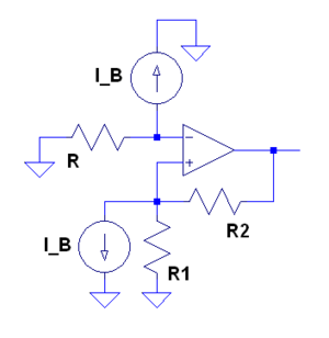
[[Image:E2.17.PNG|thumb|300px|Problem 2.17 after finishing step 4]] |
[[Image:E2.17.PNG|thumb|300px|Problem 2.17 after finishing step 4]] |
||
*Derive an expression for R in terms of the other resistor values, so that the output voltage due to the bias currents is zero. |
*Derive an expression for R in terms of the other resistor values, so that the output voltage due to the bias currents is zero. |
||
*Writing two nodal equations for each terminal voltage: <math>\frac{-V_-}{R}-I_B=0</math>, <math>-I_B+\frac{-V_+}{R_1}+\frac{-V_+}{R_2}=0</math> |
|||
*Solving the two nodal equations for the terminal voltage and then setting the two equations equal to each other gives: <math>-I_BR=-\frac{I_BR_2R_1}{R_1+R_2}</math> |
*Solving the two nodal equations for the terminal voltage and then setting the two equations equal to each other gives: <math>-I_BR=-\frac{I_BR_2R_1}{R_1+R_2}</math> |
||
*Solving for R gives: <math>R=\frac{R_2R_1}{R_1+R_2}</math> |
*Solving for R gives: <math>R=\frac{R_2R_1}{R_1+R_2}</math> |
||
| Line 46: | Line 58: | ||
<br> |
<br> |
||
<br> |
<br> |
||
<br> |
|||
<br> |
|||
==Reviewers== |
|||
*[[Ben Henry|Henry,Ben]] |
|||
*[[Lau, Chris|Christopher Garrison Lau I]] |
|||
==Readers== |
|||
*[[Lau, Chris|Christopher Garrison Lau I]] |
|||
==Amplifier Circuits== |
|||
Latest revision as of 20:05, 17 January 2010
Ideal Op Amp Characteristics
- Infinite input impedance
- Infinite open-loop gain for the differential signal
- Zero gain for the common mode signal
- You can easily change an differential amplifier into a common-mode amplifier by grounding one of the inputs
- Zero output impedance
- Infinite bandwidth
- This means there are no inductors or capacitors in the model and allows for instantaneous changes (and infinite gain regardless of frequency).
Op Amp Nodal Analysis
- No current flows into the + or - terminals
- If negative feedback is present (and no positive feedback), then
- Write nodal equations at and , but not at
- There is a voltage source inside the op amp. Writing a nodal equation at a voltage source adds an extra equation and an extra variable. It doesn't make the problem any easier.
DC imperfections
- Bias currents, and , are the average dc currents flowing into the op amp input terminals. They can be caused by the signal source, feedback resistors, etc.
- The bias current is the average of the dc currents.
- Offset current is the difference between the bias currents.
- Offset voltage occurs when the output voltage is nonzero for zero input voltage.
Canceling bias currents
- Because bias current flows have equal magnitude and direction, it is possible to negate their effects.
- The orientation of the offset voltage and the direction of the offset current are unknown, thus it is not possible to correct for these parameters with a circuit design.
Steps
- Ground the input
- Set the output to 0
- Add in the bias currents
- Add in the new resistor to balance out the bias currents
- Set the two (input terminal) nodal equations equal to each other and solve for the new resistor
Reasoning
- When the input is grounded, the bias currents will lead to an offset voltage. Arbitrarily setting the output to zero and adding in the bias resistor allows us to have current flowing through the bias resistor equal to even out the bias currents. Due to symmetry, the bias currents will cancel each other out.
Problem 2.17
- Derive an expression for R in terms of the other resistor values, so that the output voltage due to the bias currents is zero.
- Writing two nodal equations for each terminal voltage: ,
- Solving the two nodal equations for the terminal voltage and then setting the two equations equal to each other gives:
- Solving for R gives:


