Chapter 3 problems: Difference between revisions
Jump to navigation
Jump to search
(→3.17) |
(→3.17) |
||
| (10 intermediate revisions by the same user not shown) | |||
| Line 5: | Line 5: | ||
*Overlay the above two points with the diode characteristics to find the answer. |
*Overlay the above two points with the diode characteristics to find the answer. |
||
'''Part B''' |
'''Part B''' |
||
*Thevenin Equivalent: <math>V_{oc}=200*.005=1V</math> and <math>R_{th}=200+200=400</math> |
|||
*Is there a physical part that mimics the device characteristics of X? |
|||
*Using |
*Using KVL: <math>-1+400*I_B+V_X=0</math>, thus <math>V=1</math> and <math>I=0.0025</math> for the load line. |
||
*<math>I_B</math> can be read from the load line graph. We can then use this information to find the voltage over <math>V_B</math>. |
|||
*Thus: <math>I_b=.005</math> and <math>V_b=1</math>, however this is off the chart. Is this correct? |
|||
'''Part C''' |
'''Part C''' |
||
* |
*KVL & KCL: <math>I_C-V_C/500-V_C/500=0</math> and <math>-0.5+V_C+V_X=0</math>. Note that <math>I_C</math> is the same thing as <math>I_X</math> |
||
:*Thus <math>V_C=250I_C</math> and <math>V_X=1/2-250I_C</math>. Using the load line to find the I & V of device X. Then plug into the second equation to find <math>V_C</math> |
|||
*I believe there is a problem with my equation. |
|||
===3.17=== |
===3.17=== |
||
| Line 21: | Line 21: | ||
:*<math>I=0</math> and <math>V=7.5</math>. D1, D2, D3 pass. |
:*<math>I=0</math> and <math>V=7.5</math>. D1, D2, D3 pass. |
||
Check each guess please. More importantly, check the wrong assumptions. |
|||
'''Part B''' |
'''Part B''' |
||
*<math>V_{in}=0</math>, <math>V= |
*<math>V_{in}=0</math>, <math>V=5</math>: D1, D2, D3, D4 on. |
||
*<math>V_{in}=2</math>, <math>V= |
*<math>V_{in}=2</math>, <math>V=5</math>: D1, D2, D3, D4 on. |
||
*<math>V_{in}=6</math>, <math>V=5</math>: D2, D3 on. D1, D4 off. |
*<math>V_{in}=6</math>, <math>V=5</math>: D2, D3 on. D1, D4 off. |
||
*<math>V_{in}=10</math>, <math>V=5</math>: D2, D3 on. D1, D4 off. |
*<math>V_{in}=10</math>, <math>V=5</math>: D2, D3 on. D1, D4 off. |
||
*<math>V=-5</math> for <math>-10 \le V_{in} \le -5</math> |
|||
V=0. D1, D4 on. Can you really sink current into a voltage source? I don't see how you will ever have negative voltage across the diodes. |
|||
*<math>V=</math> for <math>-5 \le V_{in} \le 5</math> |
|||
*<math>V=5</math> for <math>5 \le V_{in} \le 10</math> |
|||
===3.32=== |
===3.32=== |
||
| Line 35: | Line 36: | ||
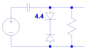
===3.33=== |
===3.33=== |
||
[[Image:P3.33.PNG|300px|none]] |
|||
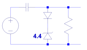
===3.37=== |
===3.37=== |
||
[[Image:P3.37.PNG|300px|none]] |
|||
===3.38=== |
|||
[[Image:P3.38.PNG|300px|none]] |
|||
Latest revision as of 17:05, 2 March 2010
3.9
Part A
- Using KVL:
- Thus the two points for the load line are and
- Overlay the above two points with the diode characteristics to find the answer.


Part B
- Thevenin Equivalent: and
- Using KVL: , thus and for the load line.
- can be read from the load line graph. We can then use this information to find the voltage over .


Part C
- KVL & KCL: and . Note that is the same thing as


- Thus and . Using the load line to find the I & V of device X. Then plug into the second equation to find


3.17
Part A
- Guessing D1 is on, D2 and D3 are off. Looking at the voltage drops, this is very unlikely.
- Guessing D1 off, D2 on, D3 off. and .


- Checking for positive current through presumed on diodes and negative voltage across the presumed off diodes.
- D1 and D2 fail. D3 passes.
- Guessing D1 and D2 on, D3 off.
- and . D1, D2, D3 pass.

Part B
- , : D1, D2, D3, D4 on.
- , : D1, D2, D3, D4 on.
- , : D2, D3 on. D1, D4 off.
- , : D2, D3 on. D1, D4 off.


- for
- for
- for


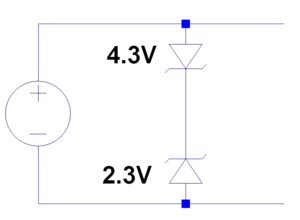
3.32
- How does this circuit work?
3.33

3.37

3.38
