Chapter 2: Difference between revisions
Jump to navigation
Jump to search
No edit summary |
|||
| Line 37: | Line 37: | ||
*Solving the two nodal equations for the terminal voltage and then setting the two equations equal to each other gives: <math>-I_BR=-\frac{I_BR_2R_1}{R_1+R_2}</math> |
*Solving the two nodal equations for the terminal voltage and then setting the two equations equal to each other gives: <math>-I_BR=-\frac{I_BR_2R_1}{R_1+R_2}</math> |
||
*Solving for R gives: <math>R=\frac{R_2R_1}{R_1+R_2}</math> |
*Solving for R gives: <math>R=\frac{R_2R_1}{R_1+R_2}</math> |
||
<br> |
|||
<br> |
|||
<br> |
|||
<br> |
<br> |
||
<br> |
<br> |
||
Revision as of 16:24, 11 January 2010
Ideal Op Amp Characteristics
- Infinite input impedance
- Infinite open-loop gain for the differential signal
- Zero gain for the common mode signal
- You can easily change an differential amplifier into a common-mode amplifier by grounding one of the inputs
- Zero output impedance
- Infinite bandwidth
- To allow for infinite gain regardless of the frequency? Instantaneous feedback?
Op Amp Nodal Analysis
- No current flows into the + or - terminals
- If negative feedback is present (and no positive feedback), then
- Write nodal equations at and , but not at
- There is a voltage source inside the op amp. Writing a nodal equation at a voltage source adds an extra equation and an extra variable. You gain no ground.
DC imperfections
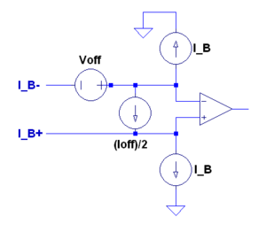
- Bias currents, and , are the average dc currents flowing into the op amp input terminals. They can be caused by the signal source, feedback resistors, etc.
- The bias current is the average of the dc currents.
- Offset current is the difference between the bias currents.
- Offset voltage occurs when the output voltage is nonzero for zero input voltage.
Canceling bias currents
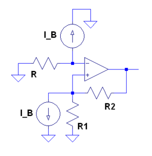
- Because bias currents flow have equal magnitude and direction, it is possible to negate their effects.
- The orientation of the offset voltage and the direction of the offset current are unknown, thus it is not possible to correct for these parameters with a circuit design.
Steps
- Ground the input
- Set the output to 0
- Add in the bias currents
- Add in the new resistor to balance out the
- Set the two nodal equations equal to each other and solve for the new resistor
Problem 2.17
- Derive an expression for R in terms of the other resistor values, so that the output voltage due to the bias currents is zero.
- Solving the two nodal equations for the terminal voltage and then setting the two equations equal to each other gives:
- Solving for R gives:


