Chapter 3 problems: Difference between revisions
Jump to navigation
Jump to search
(→3.33) |
(→3.33) |
||
| Line 35: | Line 35: | ||
===3.33=== |
===3.33=== |
||
[[Image:P3.33.PNG| |
[[Image:P3.33.PNG|300px|none]] |
||
===3.37=== |
===3.37=== |
||
Revision as of 11:32, 1 March 2010
3.9
Part A
- Using KVL:
- Thus the two points for the load line are and
- Overlay the above two points with the diode characteristics to find the answer.
Part B
- Is there a physical part that mimics the device characteristics of X?
- Using KCL:
- Thus: and , however this is off the chart. Is this correct?
Part C
- Using KCL:
- I believe there is a problem with my equation.
3.17
Part A
- Guessing D1 is on, D2 and D3 are off. Looking at the voltage drops, this is very unlikely.
- Guessing D1 off, D2 on, D3 off. and .
- Checking for positive current through presumed on diodes and negative voltage across the presumed off diodes.
- D1 and D2 fail. D3 passes.
- Guessing D1 and D2 on, D3 off.
- and . D1, D2, D3 pass.
Check each guess please. More importantly, check the wrong assumptions.
Part B Need help on this one.
- , : D1, D4 on. D2, D3 off.
- , : D1, D4 on. D2, D3 off.
- , : D2, D3 on. D1, D4 off.
- , : D2, D3 on. D1, D4 off.
V=0. D1, D4 on. Can you really sink current into a voltage source? I don't see how you will ever have negative voltage across the diodes.
3.32
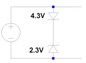
- How does this circuit work?


