Chapter 3: Difference between revisions
Jump to navigation
Jump to search
No edit summary |
|||
| Line 6: | Line 6: | ||
:*The load-line equation is obtained by applying KVL or KCL. The equation plots as a straight line that can be drawn by locating two points. |
:*The load-line equation is obtained by applying KVL or KCL. The equation plots as a straight line that can be drawn by locating two points. |
||
*In circuits with multiple diodes, it is not immediately apparent which diodes are on or off. The ideal-diode model assumes that the diode is a perfect conductor with zero voltage drop in the forward direction and an open circuit in the reverse direction. |
*In circuits with multiple diodes, it is not immediately apparent which diodes are on or off. The ideal-diode model assumes that the diode is a perfect conductor with zero voltage drop in the forward direction and an open circuit in the reverse direction. |
||
:*'''Is there a better, less exhaustive method to determine which diodes are on or off? With the current system, for n diodes there are <math>2^n</math> possibilities.''' |
|||
#Assume a set of states for the diodes |
#Assume a set of states for the diodes |
||
#Solve the circuit to find <math>i_D</math> for diodes assumed to be on and <math>v_D</math> for diodes assumed to be off |
#Solve the circuit to find <math>i_D</math> for diodes assumed to be on and <math>v_D</math> for diodes assumed to be off |
||
#Check to see if <math>i_D</math> is positive for all diodes assumed to be on and if <math>v_D</math> is negative for all diodes assumed to be off. |
#Check to see if <math>i_D</math> is positive for all diodes assumed to be on and if <math>v_D</math> is negative for all diodes assumed to be off. |
||
*Explain peak inverse voltage, PIV. |
*Explain peak inverse voltage, PIV. |
||
*'''Full-wave rectifier circuits: Center-tapped transformer & diode bridge. What are the pros and cons to each?''' |
|||
===Full Wave Recififier: Center-tapped Transformer=== |
===Full Wave Recififier: Center-tapped Transformer=== |
||
| Line 19: | Line 17: | ||
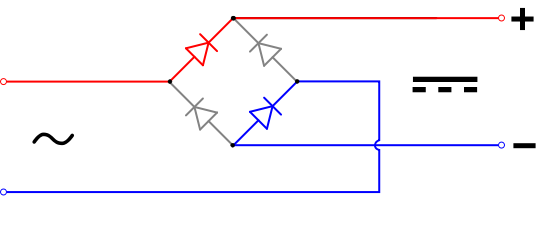
[[Image:557px-Diode_bridge_alt_1.svg.png|thumb|none|557px| ]] |
[[Image:557px-Diode_bridge_alt_1.svg.png|thumb|none|557px| ]] |
||
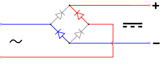
[[Image:557px-Diode_bridge_alt_2.svg.png|thumb|557px|none]] |
[[Image:557px-Diode_bridge_alt_2.svg.png|thumb|557px|none]] |
||
*The diode bridge has a larger voltage drop due to two diodes in comparison to the center-tapped transformer. |
|||
===Clipper Circuit=== |
===Clipper Circuit=== |
||
Revision as of 11:41, 2 March 2010
Diodes
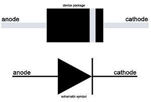
- Forward bias occurs when the P-type semiconductor material is connected to the positive terminal of a battery and the N-type semiconductor material is connected to the negative terminal, as shown below. This usually makes the p–n junction conduct. <ref> Wikipedia P-N junction</ref>
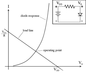
- Because diodes are a nonlinear device, traditional circuit analysis will not work on them. One method of analyze the diodes is to do it graphically. This technique is called Load-line analysis.
- The load-line equation is obtained by applying KVL or KCL. The equation plots as a straight line that can be drawn by locating two points.
- In circuits with multiple diodes, it is not immediately apparent which diodes are on or off. The ideal-diode model assumes that the diode is a perfect conductor with zero voltage drop in the forward direction and an open circuit in the reverse direction.
- Assume a set of states for the diodes
- Solve the circuit to find for diodes assumed to be on and for diodes assumed to be off
- Check to see if is positive for all diodes assumed to be on and if is negative for all diodes assumed to be off.
- Explain peak inverse voltage, PIV.
Full Wave Recififier: Center-tapped Transformer
Full Wave Recitifier: Diode Bridge
- The diode bridge has a larger voltage drop due to two diodes in comparison to the center-tapped transformer.
Clipper Circuit
- The resistor is large enough that the forward diode current is within reasonable bounds and small enough so that the reverse bias current results in a negligible voltage drop.
- A battery + diode can be used to clip the circuit. A Zener diode will often take the place of the battery in a clipper circuit.
- Placing a resistor in series with the diodes can allow for more gradual transfer characteristics.
Clamp Circuit
- The large capacitor acts as a DC offset and has a very small impedance for the AC signal. A large resistor is chosen to allow the capacitor to discharge slowly.
- Diodes are then used to define the upper and lower limit by conducting if the voltage goes outside their specified range.
- Why aren't the waveforms clipping in F3.20 (P149)
Linear Small-Signal Equivalent Circuits
- Dc supply voltages are used to bias a nonlinear device at an operating point and a small ac signal is injected into the circuit. If we consider a small enough region of operation, we can find a linear small-signal equivalent circuit.<ref>Electronics p156</ref>
- The DC supply voltage results in the circuit operating at the quiescent point. We can use this point to find the dynamic resistance of the diode.
- The analysis of nonlinear electronic circuits is often accomplished in two steps: First, the dc operating point is determined, and a linear small-signal equivalent circuit is found for the nonlinear devices; second, the equivalent circuit is analyzed. <ref>Electronics p188</ref>
- Shockley Diode equation:
- is the saturation current:
- is the thermal voltage:
- Dynamic small-signal resistance of the diode at the Q-point:
To Do
- Start up Chapter 3 problems
- Extend the bag of tricks post. Have subsections for op amps and diodes now. Then BJTs later.
References
<references/>


