Chapter 3: Difference between revisions
Jump to navigation
Jump to search
| (13 intermediate revisions by the same user not shown) | |||
| Line 3: | Line 3: | ||
[[Image:Load_line_diode.png|thumb|300px|Diode load line ]] | [[Image:Load_line_diode.png|thumb|300px|Diode load line ]] | ||
*Forward bias occurs when the P-type semiconductor material is connected to the positive terminal of a battery and the N-type semiconductor material is connected to the negative terminal, as shown below. This usually makes the p–n junction conduct. <ref> [http://en.wikipedia.org/wiki/P-n_junction#Forward_bias Wikipedia P-N junction]</ref> | *Forward bias occurs when the P-type semiconductor material is connected to the positive terminal of a battery and the N-type semiconductor material is connected to the negative terminal, as shown below. This usually makes the p–n junction conduct. <ref> [http://en.wikipedia.org/wiki/P-n_junction#Forward_bias Wikipedia P-N junction]</ref> | ||
===Load Line Analysis=== | |||
*Because diodes are a nonlinear device, traditional circuit analysis will not work on them. One method of analyze the diodes is to do it graphically. This technique is called Load-line analysis. | *Because diodes are a nonlinear device, traditional circuit analysis will not work on them. One method of analyze the diodes is to do it graphically. This technique is called Load-line analysis. | ||
*The load-line equation is obtained by applying KVL or KCL. The equation plots as a straight line that can be drawn by locating two points. | |||
*You may need to make a Thevenin or Norton equivalent before doing your load-line analysis | |||
===Ideal Diode Model=== | |||
*In circuits with multiple diodes, it is not immediately apparent which diodes are on or off. The ideal-diode model assumes that the diode is a perfect conductor with zero voltage drop in the forward direction and an open circuit in the reverse direction. | *In circuits with multiple diodes, it is not immediately apparent which diodes are on or off. The ideal-diode model assumes that the diode is a perfect conductor with zero voltage drop in the forward direction and an open circuit in the reverse direction. | ||
#Assume a set of states for the diodes | #Assume a set of states for the diodes | ||
#Solve the circuit to find <math>i_D</math> for diodes assumed to be on and <math>v_D</math> for diodes assumed to be off | #Solve the circuit to find <math>i_D</math> for diodes assumed to be on and <math>v_D</math> for diodes assumed to be off | ||
#Check to see if <math>i_D</math> is positive for all diodes assumed to be on and if <math>v_D</math> is negative for all diodes assumed to be off. | #Check to see if <math>i_D</math> is positive for all diodes assumed to be on and if <math>v_D</math> is negative for all diodes assumed to be off. | ||
*Explain peak inverse voltage, PIV. | *'''Explain peak inverse voltage, PIV.''' | ||
===Thevenin equivalent=== | |||
#Find the Thevenin source voltage by removing the load from the original circuit and calculating voltage across the open connection points where the load used to be. | |||
#Find the Thevenin resistance by removing all power sources in the original circuit (voltage sources shorted and current sources open) and calculating total resistance between the open connection points. | |||
===Full Wave Recififier: Center-tapped Transformer=== | ===Full Wave Recififier: Center-tapped Transformer=== | ||
| Line 20: | Line 26: | ||
[[Image:557px-Diode_bridge_alt_1.svg.png|thumb|none|557px| ]] | [[Image:557px-Diode_bridge_alt_1.svg.png|thumb|none|557px| ]] | ||
[[Image:557px-Diode_bridge_alt_2.svg.png|thumb|557px|none]] | [[Image:557px-Diode_bridge_alt_2.svg.png|thumb|557px|none]] | ||
*The diode bridge has a larger voltage drop due to two diodes in comparison to the center-tapped transformer. | |||
===Clipper Circuit=== | ===Clipper Circuit=== | ||
*A battery + diode can be used to clip the circuit. A Zener diode will often take the place of the battery in a clipper circuit. | *A battery + diode can be used to clip the circuit. A Zener diode will often take the place of the battery in a clipper circuit. | ||
*Placing a resistor in series with the diodes can allow for more gradual transfer characteristics. | *Placing a resistor in series with the diodes can allow for more gradual transfer characteristics. | ||
===Clamp Circuit=== | ===Clamp Circuit=== | ||
*The | *The direction of the diode will determine whether the positive or negative peaks are clamped. | ||
*The charged capacitor value will determine the value the peaks are clamped at. | |||
*Diodes are then used to define the upper and lower limit by conducting if the voltage goes outside their specified range. | *Diodes are then used to define the upper and lower limit by conducting if the voltage goes outside their specified range. | ||
===Linear Small-Signal Equivalent Circuits=== | ===Linear Small-Signal Equivalent Circuits=== | ||
Latest revision as of 14:17, 2 March 2010
Diodes
- Forward bias occurs when the P-type semiconductor material is connected to the positive terminal of a battery and the N-type semiconductor material is connected to the negative terminal, as shown below. This usually makes the p–n junction conduct. <ref> Wikipedia P-N junction</ref>
Load Line Analysis
- Because diodes are a nonlinear device, traditional circuit analysis will not work on them. One method of analyze the diodes is to do it graphically. This technique is called Load-line analysis.
- The load-line equation is obtained by applying KVL or KCL. The equation plots as a straight line that can be drawn by locating two points.
- You may need to make a Thevenin or Norton equivalent before doing your load-line analysis
Ideal Diode Model
- In circuits with multiple diodes, it is not immediately apparent which diodes are on or off. The ideal-diode model assumes that the diode is a perfect conductor with zero voltage drop in the forward direction and an open circuit in the reverse direction.
- Assume a set of states for the diodes
- Solve the circuit to find for diodes assumed to be on and for diodes assumed to be off
- Check to see if is positive for all diodes assumed to be on and if is negative for all diodes assumed to be off.
- Explain peak inverse voltage, PIV.
Thevenin equivalent
- Find the Thevenin source voltage by removing the load from the original circuit and calculating voltage across the open connection points where the load used to be.
- Find the Thevenin resistance by removing all power sources in the original circuit (voltage sources shorted and current sources open) and calculating total resistance between the open connection points.
Full Wave Recififier: Center-tapped Transformer

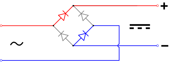
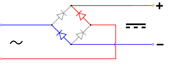
Full Wave Recitifier: Diode Bridge


- The diode bridge has a larger voltage drop due to two diodes in comparison to the center-tapped transformer.
Clipper Circuit
- A battery + diode can be used to clip the circuit. A Zener diode will often take the place of the battery in a clipper circuit.
- Placing a resistor in series with the diodes can allow for more gradual transfer characteristics.
Clamp Circuit
- The direction of the diode will determine whether the positive or negative peaks are clamped.
- The charged capacitor value will determine the value the peaks are clamped at.
- Diodes are then used to define the upper and lower limit by conducting if the voltage goes outside their specified range.
Linear Small-Signal Equivalent Circuits
- Dc supply voltages are used to bias a nonlinear device at an operating point and a small ac signal is injected into the circuit. If we consider a small enough region of operation, we can find a linear small-signal equivalent circuit.<ref>Electronics p156</ref>
- The DC supply voltage results in the circuit operating at the quiescent point. We can use this point to find the dynamic resistance of the diode.
- The analysis of nonlinear electronic circuits is often accomplished in two steps: First, the dc operating point is determined, and a linear small-signal equivalent circuit is found for the nonlinear devices; second, the equivalent circuit is analyzed. <ref>Electronics p188</ref>
- Shockley Diode equation:
- is the saturation current:
- is the thermal voltage:
- Dynamic small-signal resistance of the diode at the Q-point:
To Do
- Start up Chapter 3 problems
- Extend the bag of tricks post. Have subsections for op amps and diodes now. Then BJTs later.
References
<references/>