Chapter 4: Difference between revisions
Jump to navigation
Jump to search
| Line 88: | Line 88: | ||
:*Coupling capacitor to separate the AC input/output from the DC biasing |
:*Coupling capacitor to separate the AC input/output from the DC biasing |
||
:*Bypass capacitor allows for a common-emitter for AC, yet provides a stable bias current for DC |
:*Bypass capacitor allows for a common-emitter for AC, yet provides a stable bias current for DC |
||
*Voltage gain: |
|||
| ⚫ | |||
:*<math>v_{in}=i_b r_\pi + (\beta + 1)i_b R_{E1}\,</math> |
|||
| ⚫ | |||
:*<math>v_o=\beta i_b R^'_L\,</math> |
|||
:*The direction of the current necessitates the minus sign |
|||
| ⚫ | |||
:*If <math>(\beta+1)R_{E1}\gg R_\pi</math> and <math>\beta \gg 1</math> then <math>A_v \cong -\frac{R^'_L}{R_{E1}}</math> and the gain is nearly independent of the transistor parameters. |
:*If <math>(\beta+1)R_{E1}\gg R_\pi</math> and <math>\beta \gg 1</math> then <math>A_v \cong -\frac{R^'_L}{R_{E1}}</math> and the gain is nearly independent of the transistor parameters. |
||
| ⚫ | |||
*Input Impedance: |
|||
*Input Impedance: '''How do they get v_in (E4.45)? Why is v_o dependent on R^'_L instead of just R_L?''' |
|||
*Current Gain & Power Gain: |
*Current Gain & Power Gain: |
||
*Output Impedance: |
*Output Impedance: |
||
*Make sure you can run through Example 4.9 |
|||
<br> |
|||
<br> |
|||
<br> |
|||
<br> |
|||
<br> |
|||
<br> |
|||
<br> |
|||
<br> |
|||
<br> |
|||
<br> |
|||
<br> |
|||
<br> |
|||
<br> |
|||
<br> |
|||
===BJT models?=== |
===BJT models?=== |
||
Revision as of 10:21, 8 March 2010
Bipolar Junction Transistor
How a BJT works
- NPN: Not Pointing iN
- PNP: Pointing iN Please
- The arrow is for the emitter current.
- For an NPN the current flows into the collector. For a PNP the current flows out of the collector.
- Quiescent is a none referring to a state of being quiet, still, at rest, dormant, inactive. In an electronic amplifier or filter is said to be in a quiescent state when no signal is applied to its input
| DC sources | AC sources | Capacitor | BJT | |
|---|---|---|---|---|
| DC analysis | No change | 0V or 0A | Open-Circuit | Active, Saturation or Cutoff |
| AC analysis | 0V or 0A | No change | Short-Circuit | Small-signal model |
Signal Notation
- Total =
- DC =
- AC =
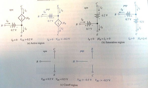
Large-Signal DC models
|
|
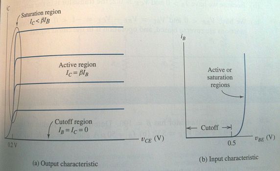
- Active: The normal mode of operation. This mode has the largest common-emitter current gain.
- Reverse Active: The collector and emitter roles are reversed. Most BJTs are not symmetrical, thus and take on different values.
- Saturation: High current from the emitter to collector. Logical "on".
- Cutoff: Very little current flow. Logical "off".
Large-Signal DC Analysis
- Assume an operating region for the BJT.
- Solve the circuit to find
- Check the values to see if they match the region constraints.
Bias-Circuit Design
- The principle goal of bias-circuit design is to achieve nearly identical operating points for the BJTs, even though the BJT parameters may vary significantly from unit to unit. <ref>Electronics p245</ref>
- Fixed-base bias circuit is a very simplistic method that does not deal well with a wide variety of values. The base current does not adjust for changes in . If you want a circuit that has a particular operating point on the collector load line, the base current must change with .
- Using two voltage sources (one for the collector and one for the base) achieves an emitter current that is relatively independent of . Usually only one source is available or we may wish to inject a signal into the base. In an ideal world you could simply place the voltage sources in series. Since the voltage sources are grounded, they would be put in parallel. The wire connecting the voltage source will see the potential difference (and a lot of current). The wire will burn up and bad things will happen to the voltage sources.
- Four-resistor bias circuit provides a constant base voltage independant of . This design is great for discrete circuits, but is impractical in integrated circuits because of the excessive chip area they consume.
- How does this handle injecting an ac source? How is it not coupled?
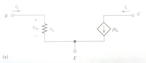
Small-Signal Equivalent Circuits
- Tranconductance:
Common-Emitter Amplifier
- A four-resistor biasing network
- Coupling capacitor to separate the AC input/output from the DC biasing
- Bypass capacitor allows for a common-emitter for AC, yet provides a stable bias current for DC
- Voltage gain:
- Why don't they use R1 & R2 when finding Vin?
- The direction of the current necessitates the minus sign
- If and then and the gain is nearly independent of the transistor parameters.
- Input Impedance:
- Current Gain & Power Gain:
- Output Impedance:
BJT models?
| Type? | Input Resistance | Output Resistance | Gain | Frequency response |
|---|---|---|---|---|
| Common-emitter | ||||
| Common-collector | ||||
| Common-base |
Questions
- Why do we always seem to use a common emitter configuration? Common-base and common-collector have different properties.
- For P3.17 make the glob of sauder assuming they're all on and check the currents running through each one. Make sure they go the right way, and add up?
- Why is the input/output impedance so important?
- P4.54c
References
<references/>


