Chapter 5: Difference between revisions
Jump to navigation
Jump to search
| Line 19: | Line 19: | ||
|} |
|} |
||
{| class="wikitable" border="1" style="text-align:center" |
|||
|+ '''Alternate method''' |
|||
! Region!! <math>v_{GS}\,</math> !! <math>v_{DS}\,</math> |
|||
|- |
|||
| Cutoff|| <math>v_{GS}<V_{to}\,</math> |
|||
|- |
|||
| Triode|| <math>v_ |
|||
|- |
|||
| Saturation |
|||
|} |
|||
Determining the Operating Region |
Determining the Operating Region |
||
Revision as of 14:43, 19 March 2010
NMOS Transistor
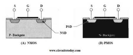
- N-channel enhancement-mode MOSFET (metal-oxide semiconductor field effect transistor)
| Region | |||
|---|---|---|---|
| Cutoff | 0 | ||
| Triode | |||
| Saturation | |||
| Boundry | |||
| Region | |||||||||||||||||||||||||
|---|---|---|---|---|---|---|---|---|---|---|---|---|---|---|---|---|---|---|---|---|---|---|---|---|---|
| Cutoff | |||||||||||||||||||||||||
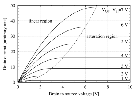
| Triode | Failed to parse (syntax error): {\displaystyle v_ |- | Saturation |} Determining the Operating Region *Cutoff: If V<sub>GS</sub> is less than V<sub>to</sub> *Triode: If not Cutoff and V<sub>DG</sub> is less than V<sub>to</sub> *Saturation: If not Cutoff or Triode Determining V<sub>to</sub> *Enhancement: Build the channel *Depletion: Pinch-off the channel *JFET: Pinch-off the channel *'''Triode:''' :*The threshold voltage, <math>V_{to}}
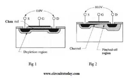
, is the minimum needed to move the transistor from the Cutoff to Triode region. When is reached, a channel forms beneath the gate, allowing current to flow.
MOSFET analysis
Small-signal equivalent circuits
Questions
References<references/> |


![{\displaystyle K[2(v_{GS}-V_{to})v_{DS}-v_{DS}^{2}]}](https://wikimedia.org/api/rest_v1/media/math/render/svg/40bb5b0ffa3dcb84c09c7252ed8fc731f03619f2)


